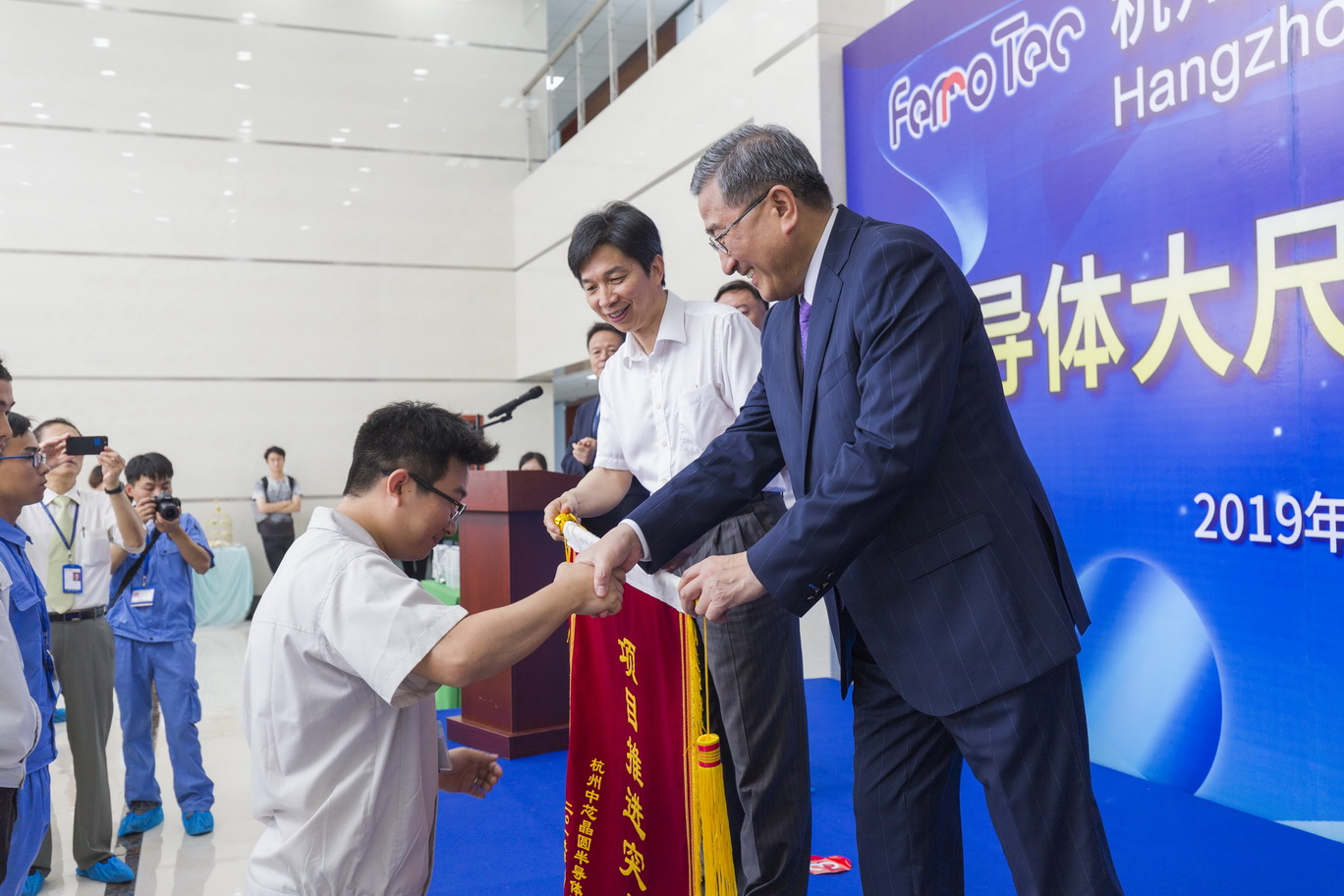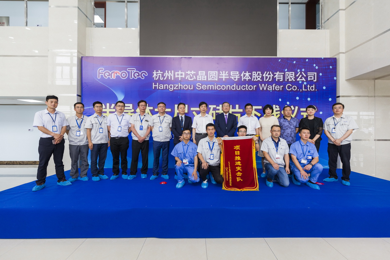


April showers bring May flowers. Ferrotec (China) Hangzhou semiconductor wafer Co., Ltd. (hereinafter referred to as "FTHW") after 16 months of "semiconductor large-scale silicon chip project" finally ushered in the first batch of products in the market yesterday.
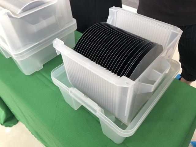
This is also the first batch of 8-inch (200 mm) semiconductor silicon polishing chips in Hangzhou, which means that FTHW has made a big step forward in promoting the chip design and manufacturing industry in Hangzhou.

FTHW is jointly invested by Japan Magnetic Technology Holding Co., Ltd., Hangzhou Dahe thermal-magnetic Co., Ltd. and Shanghai Shenhe thermal-magnetic Electronics Co., Ltd. for 1 billion US dollars. The project includes three 8-inch (200 mm) and two 12 inch (300 mm) semiconductor wafer production lines, which can achieve an annual production capacity of 4.2 million 8-inch and 2.4 million 12 inch semiconductor wafers.
The construction of the project was started in February 2018, the main plant was capped in October 2018, and the production conditions were met in June 2019. It took 8 months to complete the main capping and 16 months to put into production. During the construction of the project, it has received the full support and "Butler" service from all departments at all levels of the province, the city and the new area, and really created the "Hangzhou speed" of large-scale silicon wafer project. After the first batch of 8-inch semiconductor silicon wafers are rolled off the production line, FTHW plans to achieve a mass production of 100000 large silicon wafers in October 2019, 250000 in January next year, 350000 in April, with an annual estimated sales revenue of 5 billion yuan and an annual new tax revenue of 400 million yuan.

In recent years, with the development of the new generation of information technology in the fields of artificial intelligence, big data, Internet of things, AR / VR, wearable devices, etc., China's semiconductor industry has entered a new boom cycle again, and the market demand for semiconductor wafers has increased greatly. Semiconductor wafer accounts for nearly 30% of the demand in wafer manufacturing materials, which is the most in demand. However, the supply capacity of large-scale semiconductor wafer in China is really worrying.
As a major semiconductor project of 6 billion yuan, FTHW is committed to becoming a benchmarking enterprise for independent production of large-scale semiconductor silicon wafers. "The first batch of 8-inch semiconductor silicon wafers to go offline means that the largest and most mature production line of large-scale silicon wafers in China will be produced here. In the second quarter of next year, it will reach the scale of 350000 pieces per month to fill the industry's short board." Xu Xinhua, vice general manager of FTHW, said that in order to alleviate the current situation of insufficient supply in the domestic 8-inch and 12 inch wafer markets, improve the current situation of China's semiconductor industry being stuck in the neck, and ensure the safety of silicon wafer supply in the domestic market and the integrity and stability of the integrated circuit industry chain, FTHW will be quick to achieve the mass production of 8 / 12 inch wafer as soon as possible.